Meraki MX84 Teardown and Hardware info
Teardown:
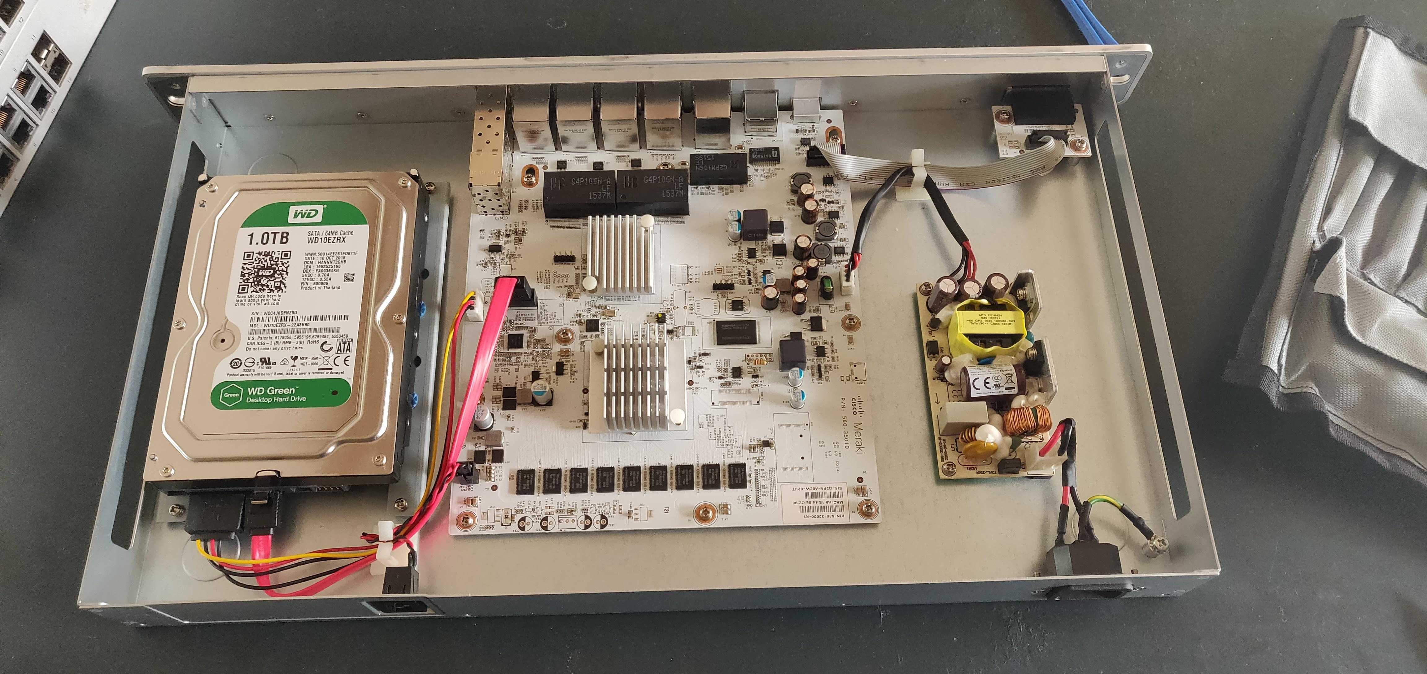 Popping the lid off this thing follows the same pattern as a lot of rack mount gear, just four screws on the back, and
the cover can slide a small amount back, then taken off completely. This unveils really cleanly laid out internals with
nearly everything screwed to the bottom of the case on standoffs.
Popping the lid off this thing follows the same pattern as a lot of rack mount gear, just four screws on the back, and
the cover can slide a small amount back, then taken off completely. This unveils really cleanly laid out internals with
nearly everything screwed to the bottom of the case on standoffs.
Hacking:
Naturally start with the easiest thing first, the 1tb HDD. Aaaand—nothing, it's a LUKS encrypted partition which is useless to us until we can get the (hopefully random) key off the system firmware.
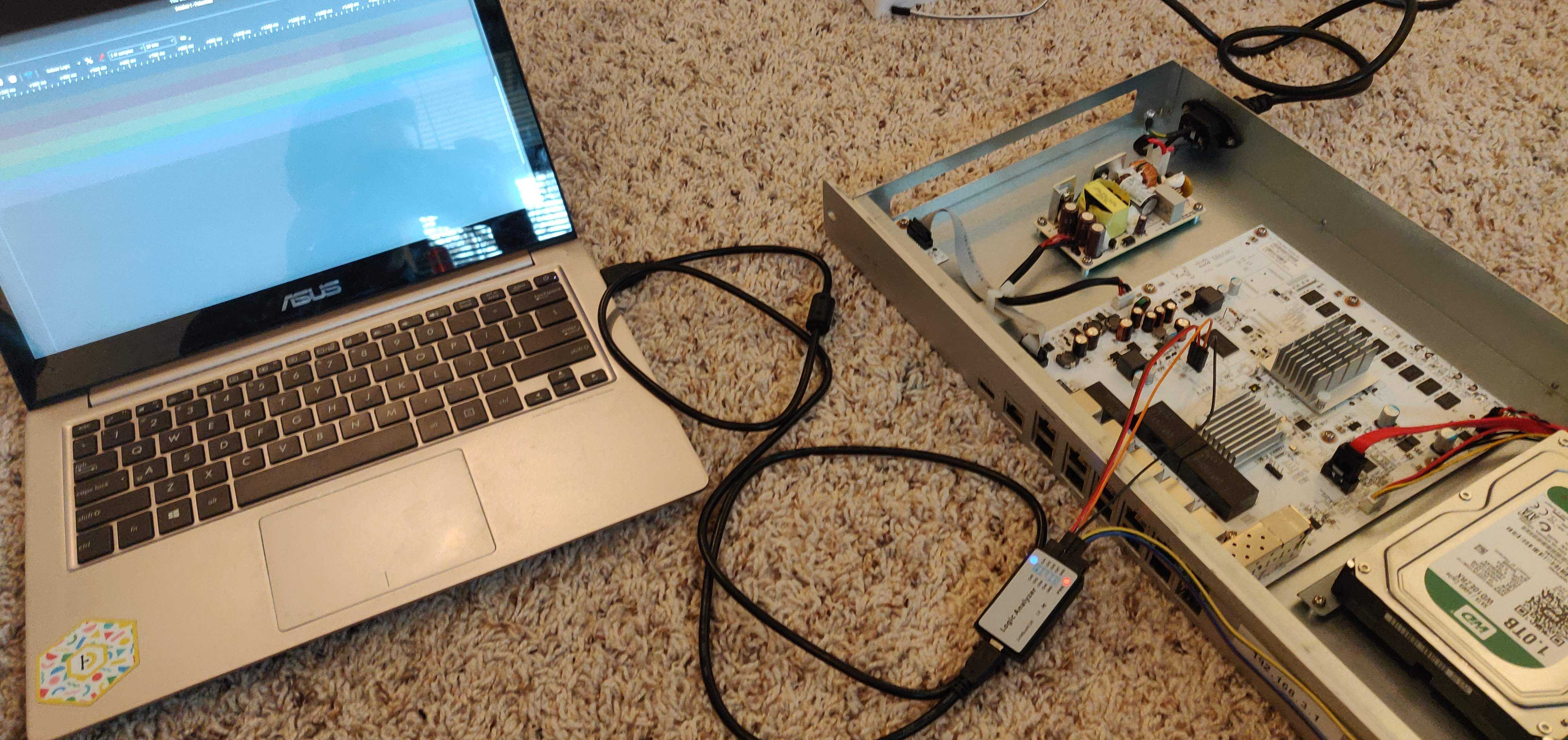 Next step, four pins! This usually means UART, the board has two headers kindly installed for us. We'll confirm with a
cheap logic analyzer and pulseview for sigrok.
Next step, four pins! This usually means UART, the board has two headers kindly installed for us. We'll confirm with a
cheap logic analyzer and pulseview for sigrok.
 Sure enough it's a 115200 baud UART connection, here's the output from my USB to TTL cable that I captured while the
system booted.
Sure enough it's a 115200 baud UART connection, here's the output from my USB to TTL cable that I captured while the
system booted.
In summary, it's a pretty standard coreboot setup with lzma/squashfs running an old version of busybox. I assume Cisco has kept stuff up to date, I just have no way to update the firmware without an admin panel. Other than that there's some hardware info, we know it's running Snort and a custom kernel, but nothing too out of the ordinary.
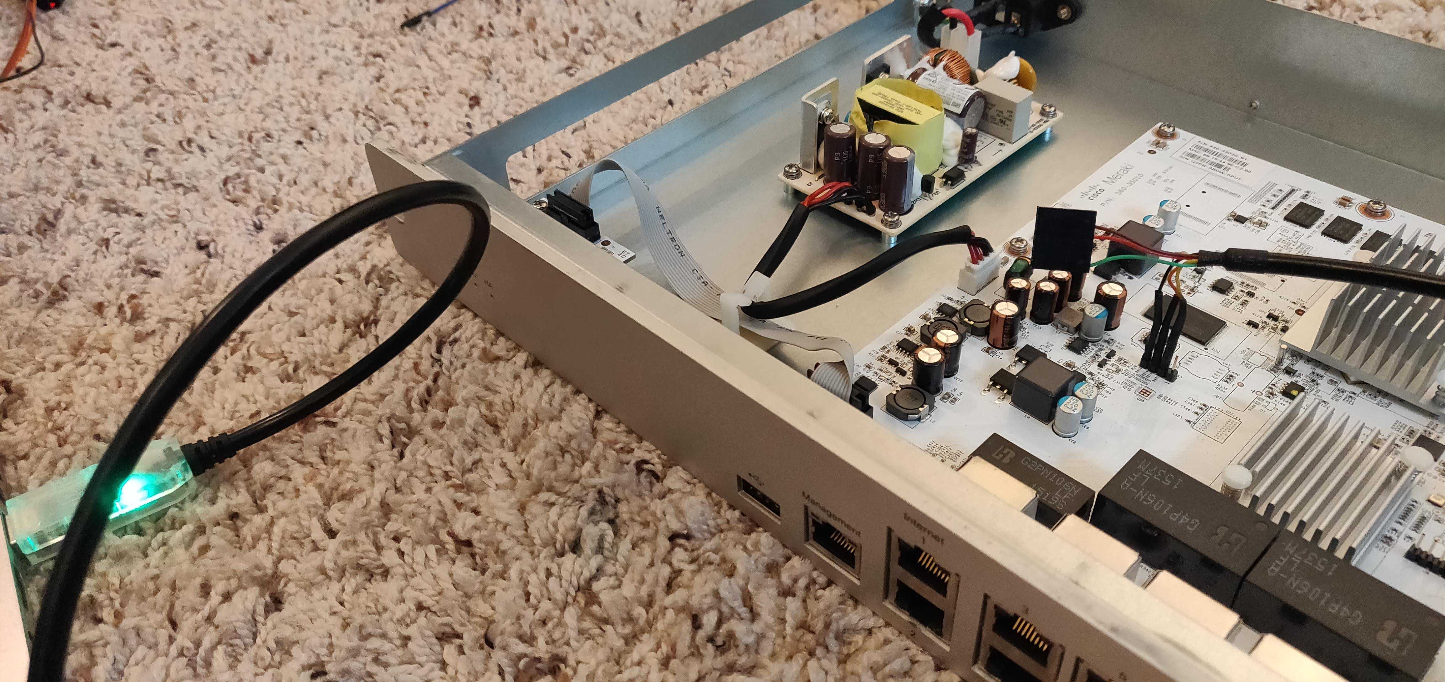
The other 4-pin header I suspect is for UART on the other chip which I'm not too concerned about right now. I think I tested it and got no output, but I'm writing this a while after I actually did all this and don't remember.
Info:
I'll go over each component on the main board one by one.
CPU
 Intel Atom C2358 - seems like an appropriate choice for this, low power embedded
More info:
https://ark.intel.com/content/www/us/en/ark/products/77978/intel-atom-processor-c2358-1m-cache-1-70-ghz.html
RAM
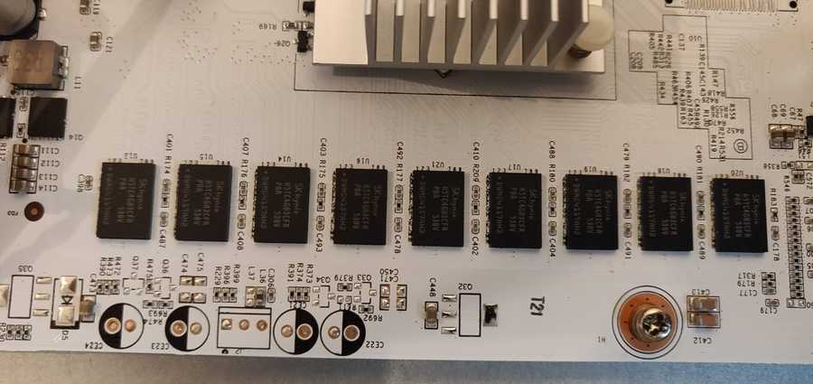 32gb of SKHynix ECC DDR3-1600
9 chips tells us it's ECC, chip number is H5TC4G83CFR, "PBA" variant
More info:
https://www.skhynix.com/products.view.do?vseq=1340&cseq=74
Ethernet controller
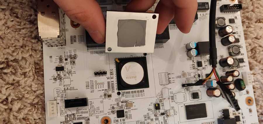 Probably the most specialized component on this board, basically a managed switch in chip form, communicates with the
CPU over some form of API. I'll leave any further investigation until the rest of the system is pwned.
Probably the most specialized component on this board, basically a managed switch in chip form, communicates with the
CPU over some form of API. I'll leave any further investigation until the rest of the system is pwned.
More info:
https://www.microsemi.com/product-directory/ethernet-switches/3969-vsc7425
Flash
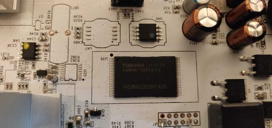 The 48 pin TFSOP is a flash chip, and likely what the system boots from, I want whatever is on it.
https://www.digikey.com/product-detail/en/toshiba-memory-america-inc/TH58NVG3S0HTA00/TH58NVG3S0HTA00-ND/5226335
The 48 pin TFSOP is a flash chip, and likely what the system boots from, I want whatever is on it.
https://www.digikey.com/product-detail/en/toshiba-memory-america-inc/TH58NVG3S0HTA00/TH58NVG3S0HTA00-ND/5226335
USB Flash controller
 Following the traces from the NAND flash chip leads to the other side of the board which houses a Phison ps2303q USB
flash controller. This is basically the chip you would find on usb drives that manages a single raw NAND flash chip.
This is how the Intel CPU communicates with the flash chip and is probably the easiest way to approach getting a
firmware dump from it. Actual info about this chip is pretty limited, when I was first working on this project I ran
into this pinout info which luckily I saved locally since the source has disappeared.
Following the traces from the NAND flash chip leads to the other side of the board which houses a Phison ps2303q USB
flash controller. This is basically the chip you would find on usb drives that manages a single raw NAND flash chip.
This is how the Intel CPU communicates with the flash chip and is probably the easiest way to approach getting a
firmware dump from it. Actual info about this chip is pretty limited, when I was first working on this project I ran
into this pinout info which luckily I saved locally since the source has disappeared.
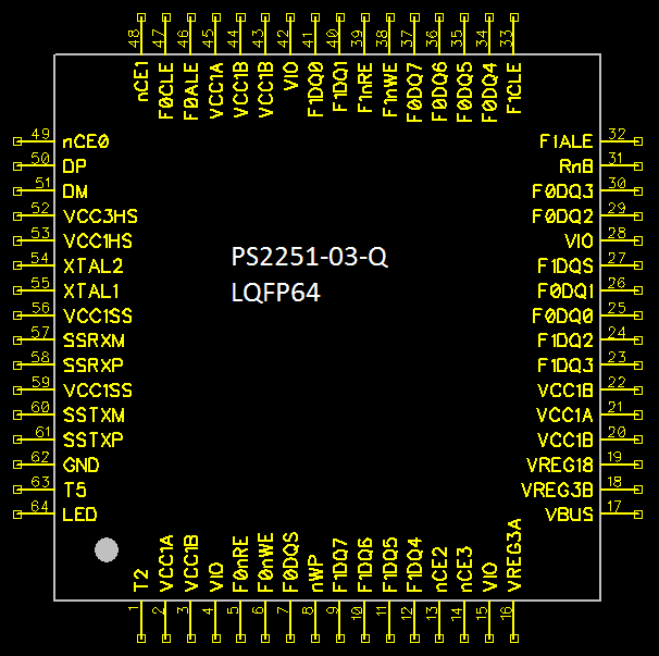
| Pin | Name | Type | Description |
|---|---|---|---|
| 1 | T2 | I,PU | Write protect switch input. 0-protect, 1-no protect |
| 2 | VCC1A | P | 1V power rail A |
| 3 | VCC1B | P | 1V power rail B (core ?) |
| 4 | VIO | P | NAND IO power rail. Connect to 3.3V or 1.85V supply |
| 5 | F0nRE | O | NAND channel 0 read enable |
| 6 | F0nWE | O | NAND channel 0 write enable |
| 7 | F0DQS | IO | NAND channel 0 data strobe |
| 8 | nWP | O | NAND common write protect |
| 9 | F1DQ7 | IO | NAND channel 1 data 7 |
| 10 | F1DQ6 | IO | NAND channel 1 data 6 |
| 11 | F1DQ5 | IO | NAND channel 1 data 5 |
| 12 | F1DQ4 | IO | NAND channel 1 data 4 |
| 13 | nCE2 | O | NAND chip enable 2 |
| 14 | nCE3 | O | NAND chip enable 3 |
| 15 | VIO | P | NAND IO power rail. Connect to 3.3V or 1.85V supply |
| 16 | VREG3A | P | 3V regulator A output. Connect to VCC3HS |
| 17 | VBUS | P | VBUS 5V input to all regulators |
| 18 | VREG3B | P | 3.3V regulator B output. Can be used to supply 3.3V VIO |
| 19 | VREG18 | P | 1.85V regulator output. Can be used to supply 1.8V VIO |
| 20 | VCC1B | P | 1V power rail B (core ?) |
| 21 | VCC1A | P | 1V power rail A |
| 22 | VCC1B | P | 1V power rail B (core ?) |
| 23 | F1DQ3 | IO | NAND channel 1 data 3 |
| 24 | F1DQ2 | IO | NAND channel 1 data 2 |
| 25 | F0DQ0 | IO | NAND channel 0 data 0 |
| 26 | F0DQ1 | IO | NAND channel 0 data 1 |
| 27 | F1DQS | IO | NAND channel 1 data strobe |
| 28 | VIO | P | NAND IO power rail. Connect to 3.3V or 1.85V supply |
| 29 | F0DQ2 | IO | NAND channel 0 data 2 |
| 30 | F0DQ3 | IO | NAND channel 0 data 3 |
| 31 | RnB | I | NAND common ready/busy |
| 32 | F1ALE | O | NAND channel 1 address latch enable |
| 33 | F1CLE | O | NAND channel 1 command latch enable |
| 34 | F0DQ4 | IO | NAND channel 0 data 4 |
| 35 | F0DQ5 | IO | NAND channel 0 data 5 |
| 36 | F0DQ6 | IO | NAND channel 0 data 6 |
| 37 | F0DQ7 | IO | NAND channel 0 data 7 |
| 38 | F1nWE | O | NAND channel 1 write enable |
| 39 | F1nRE | O | NAND channel 1 read enable |
| 40 | F1DQ1 | IO | NAND channel 1 data 1 |
| 41 | F1DQ0 | IO | NAND channel 1 data 0 |
| 42 | VIO | P | NAND IO power rail. Connect to 3.3V or 1.85V supply |
| 43 | VCC1B | P | 1V power rail B (core ?) |
| 44 | VCC1B | P | 1V power rail B (core ?) |
| 45 | VCC1A | P | 1V power rail A |
| 46 | F0ALE | O | NAND channel 0 address latch enable |
| 47 | F0CLE | O | NAND channel 0 command latch enable |
| 48 | nCE1 | O | NAND chip enable 1 |
| 49 | nCE0 | O | NAND chip enable 0 |
| 50 | DP | IO | USB D+ |
| 51 | DM | IO | USB D- |
| 52 | VCC3HS | P | USB transceiver 3V supply. Connect to VREG3A |
| 53 | VCC1HS | P | USB transceiver 1V supply. Connect to VCC1A |
| 54 | XTAL2 | C | External crystal. Leave unconnected to use internal oscillator |
| 55 | XTAL1 | C | External crystal. Leave unconnected to use internal oscillator |
| 56 | VCC1SS | P | USB SS transceiver 1V supply. Connect to VCC1A |
| 57 | SSRXM | I | USB SS RX- |
| 58 | SSRXP | I | USB SS RX+ |
| 59 | VCC1SS | P | USB SS transceiver 1V supply. Connect to VCC1A |
| 60 | SSTXM | I | USB SS TX- |
| 61 | SSTXP | I | USB SS TX+ |
| 62 | GND | P | Ground |
| 63 | T5 | ? | Test 5 pin. Leave unconnected |
| 64 | LED | O | LED control |
Conclusion
Theoretically all it should take to get a ROM off this is to hook up VBUS on pin 17, GND on pin 62, and pins 50/51 to D+ and D- on a usb 2 cable. Unfortunately this chip is painfully small which is why I've procrastinated on this project. Hopefully I get bored enough to try it soon and get a firmware dump to poke at in a kali instance. Until then, good luck to anyone who pursues this, and update me on any findings!